⚙️ The New Industrial Revolution Is Underway
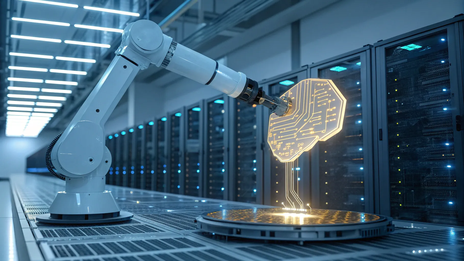
I believe we are at the start of a new industrial revolution driven by AI supercomputing. This is not incremental change. It is a transformation with a total addressable market in the trillions. The dynamics are simple in concept and staggering in scale in execution: electricity powers factories, and now AI factories will transform energy into intelligence. Physical AI will change how every manufacturing facility and warehouse operates, and every building will begin orchestrating fleets of autonomous robots, sensors, and real-time control systems.
The semiconductor industry sits at the heart of this shift. Chips enable AI; AI optimizes chip design and manufacturing. That feedback loop creates a virtuous cycle: better chips produce more powerful AI, and better AI accelerates the creation of better chips. Capturing the value of that cycle requires continuous innovation across the entire semiconductor value chain—from materials and energy efficiency to device physics, design tools, and factory processes.
I want to make clear what I mean when I talk about impact. These are not small optimizations. Across a range of semiconductor workloads we are seeing speedups from accelerated computing and AI that are measured in tens to hundreds of times. Those improvements are not just academic; they shorten design cycles, reduce cost, increase yield, and unlock entirely new capabilities like photorealistic digital twins and agentic assistants for engineers.
🔬 What AI Supercomputing and AI Infrastructure Really Mean
AI infrastructure is complex and multi-layered. It starts with land, power, and shell and extends through the hardware stack—CPUs, GPUs, DPUs, NICs, switches, memory, storage—and culminates in software libraries, APIs, and orchestration layers. Each layer must work together to deliver performant, reliable AI systems at scale.
I often describe this as a systems problem, not a single-component problem. A modern AI system is the product of global supply chains, advanced packaging, high-speed networking, and tightly optimized software. The moment you pull one thread—computation, cooling, networking—you find dependencies across the entire stack. That complexity is why partnerships across the semiconductor ecosystem matter so much.
“Blackwell is an engineering marvel.” It begins as a blank silicon wafer. Hundreds of chip processing and ultraviolet lithography steps build up each of the 200 billion transistors… From around the world, parts arrive to be assembled by skilled technicians into a rack-scale AI supercomputer. In total, 1.2 million components… Blackwell is more than a technological wonder. It is a testament to the power of global collaboration and innovation.
That passage captures the essence of modern AI hardware: intricate manufacturing, billions of transistors, miles of cables, and thousands of collaborators. Building AI infrastructure at scale is an engineering feat that requires both manufacturing excellence and profound software innovation.
🚀 CUDA-X and Libraries: The Software That Multiplies Hardware
Accelerated computing is not simply about faster chips. It is about providing software building blocks that let entire industries harness GPU acceleration without reinventing the wheel. My strategy for bringing accelerated computing to new domains has always been to build libraries of common APIs and optimized kernels: a platform that solution providers can adopt and extend.
CUDA-X is the foundation of that strategy. It includes libraries and frameworks for signal processing, computational physics, quantum-classical workflows, and more. For semiconductor workflows this matters because the same low-level primitives—matrix factorizations, linear solves, FFTs, sparse solvers—appear in many different tools. By accelerating those primitives, entire toolchains get much faster.
In semiconductor design and manufacturing we are already seeing libraries such as warp, coopt, co-DSS, and co-Litho adopted across partners. These libraries cover workloads from computational lithography to device physics to inspection and TCAD. The performance gains we are observing range from 20x to over 100x in certain workloads when tools are integrated with CUDA-X libraries.
Two examples are worth calling out in detail.
- CUDA SS. This library optimizes core routines common to many engineering computations—direct solvers, matrix reorderings, and factorization kernels. It is relatively new but rapidly adopted by large players such as Applied Materials, Cadence, Samsung, Synopsys, and TSMC. The impact is dramatic: kernels that used to take minutes can now run tens or hundreds of times faster.
- co-Litho. Computational lithography is one of the most computationally intensive pieces of the semiconductor flow. co-Litho provides GPU-accelerated building blocks for lithography simulation and optimization. We have partnered with foundries and EDA companies to optimize those pipelines, enabling much faster turnarounds for mask synthesis and verification.
Software multiplication of hardware matters because it lowers the marginal cost of innovation for every company in the ecosystem. Faster simulations mean more design iterations, higher yields, and quicker time to market.
🧠 AI Physics and Physics Nemo: Enforcing the Laws of Nature in Models
One of the central trends I am watching closely is the rise of AI physics. Traditional machine learning often treats phenomena as purely statistical. AI physics embeds physical constraints and domain knowledge directly into models so they are more accurate, interpretable, and reliable for engineering applications.
To support that, we developed Physics Nemo, a framework that sits on top of PyTorch and provides APIs to enforce physics constraints during model training. Physics Nemo is highly GPU optimized and open source, which means engineers familiar with PyTorch can leverage it to build physics-aware models quickly.
Where can AI physics make a difference in semiconductor workflows? Practically everywhere:
- Thermal analysis and stress analysis
- Computational fluid dynamics for cooling and airflow
- Computational lithography and mask synthesis
- Power and timing analysis for physical signoff
- Molecular dynamics and material modeling for device innovation
AI physics is particularly powerful when integrated into multi-physics stacks such as TCAD. TCAD workflows combine electrostatics, molecular dynamics, electromagnetics, flow dynamics, and topography. Embedding physics-aware neural networks in those pipelines yields faster simulations with fidelity that engineers can trust. In one example, TCAD workloads accelerated with a mix of libraries and AI physics have produced up to 100x end-to-end improvements in runtime for certain tasks.
That kind of speedup is not just about checking a box. It changes what teams can do day to day. Faster iterations mean deeper exploration of design spaces, leading to more robust devices and higher yield in production.
🤖 Agentic AI: Multiplying Engineer Productivity
Agentic AI will transform how engineers work. These are not mere assistants; they are autonomous agents that can orchestrate toolchains, generate and validate designs, debug physical systems, and even propose experiments. When properly integrated into engineering platforms, agentic workflows can accelerate design cycles and democratize expertise across organizations.
Several EDA and manufacturing companies are building agentic platforms that are purpose-built for semiconductor workflows:
- Cadence Jet AI powers AI-enhanced design tools across domains including digital and analog design, verification, debug, PCB layout, multi-physics optimization, and data center operations. It aims to bring AI into every stage of the engineering workflow.
- Siemens Hughes AI is focusing on automated workflows and photorealistic digital twins to improve collaboration and precision in EDA.
- Synopsys is building next-generation agentic AI platforms that combine GPU acceleration, generative AI, and autonomous agents to speed up engineering processes and make advanced tools more accessible.
In my view, agentic AI will act as a force multiplier. Engineers will still make judgement calls and set strategy, but agents will do the heavy lifting: running simulations, proposing parameter sweeps, synthesizing results into actionable recommendations, and instructing robotic systems in the factory. That combination of human creativity and agent-driven throughput will reshape productivity.
🏭 Digital Twins and the Omniverse Blueprint for AI Factories
Digital twins are the third computer in the robotics story I often tell. If you are building a physical AI—a robot or automated system—you need three interactive computers:
- A training computer to train the AI models.
- A computer in the robot to run inference and control in real time.
- A simulation computer to model the environment with physics fidelity so you can validate, test, and iterate safely before deploying into the real world.
The simulation computer is where digital twins become indispensable. Digital twins model entire factories, test beds, and production lines, enabling teams to plan layouts, validate mechanical interfaces, debug thermal and power interactions, and pre-train robots in realistic virtual environments.
“The Omniverse Blueprint for AI Factory Digital Twins enables us to design and optimize these AI factories long before physical construction starts. We integrate 3D and layout data of superpods and advanced power and cooling systems, simulate air and liquid cooling systems, and run large-scale what-if scenarios in seconds versus hours.”
That quote underscores two critical benefits: collaboration and speed. Digital twins break down silos. Mechanical engineers, controls engineers, facilities teams, and suppliers can work in parallel in a synchronized virtual environment. Decisions that used to take weeks of back-and-forth can be evaluated by running large-scale scenarios in seconds.
There are concrete, high-impact applications of factory digital twins in the semiconductor world:
- Facility planning: Generate a full 3D layout of a fab from CAD, evaluate routing, piping, and material handling prior to construction.
- Cooling and power optimization: Simulate air and liquid cooling and power distribution to maximize efficiency and minimize downtime.
- Robot training: Use the digital twin as a gym to develop, train, and validate robot manipulators, AMRs, and vision AI agents before they touch physical hardware.
- Remote monitoring and inspection: Combine sensor data with the twin to enable predictive maintenance and reduce inspection time.
- Retrofits and upgrades: Test changes in the twin to estimate downtime and cost before implementing them on the factory floor.
Large manufacturers and ODMs are already using these capabilities. Examples include TSMC for layout generation and simulation, Pegatron simulating solder paste dispensing to reduce defects, and major contract manufacturers using digital twins to plan new facilities and production lines virtually, saving millions in execution costs.
🔗 Collaboration and the Virtuous Cycle with Ecosystem Partners
One recurring theme in my work is that no single company can do this alone. Progress depends on close collaboration between EDA vendors, equipment manufacturers, foundries, systems integrators, and software providers. The breakthroughs come when these partners align on common APIs, optimized libraries, and validated workflows.
A good example is the collaboration with LAM Research. By adopting accelerated computing technologies, LAM speeds up device-level research and process development. Those improvements in tool performance then feed back into the AI and software platform, enabling us to build even more capable infrastructure. It is a truly symbiotic cycle where each participant raises the ceiling for the others.
We see similar collaborative relationships across the industry: Applied Materials, Cadence, KLA, Lam Research, Siemens, Synopsys, Samsung, and TSMC are all moving toward integrated stacks that combine domain expertise with GPU acceleration and AI physics. That combination—domain expertise plus accelerated computing—drives the most meaningful improvements.
📈 Practical Impacts: TCAD, Yield, and Manufacturing Throughput
To understand the practical value of these innovations, consider a few measurable impacts.
TCAD acceleration. TCAD workflows are multi-physics and highly compute bound. By combining CUDA-X libraries with physics-aware models, teams have reported up to 100x improvements in critical simulation tasks. That transforms the cadence of development: what used to take weeks can happen in hours or minutes, enabling more extensive parametric sweeps and more aggressive optimization strategies.
Inspection and yield optimization. Vision AI and generative models can dramatically reduce the time and cost of wafer inspection. Automated agents can flag anomalies, prioritize review queues, and guide repair or sort strategies. These advances translate directly into higher yield and lower scrap rates.
Factory bring-up and retrofits. The Omniverse Blueprint for AI factories lets teams plan and simulate complex mechanical, electrical, and cooling systems before physical assembly. Real-time simulation and collaborative planning reduce execution errors and accelerate time to bring-up. That matters enormously when bringing up facilities that house megawatt-scale compute pods.
Robotics and material handling. Pre-training robots in a high-fidelity digital twin reduces deployment risk. Robots trained in the twin can transfer learned behaviors to the real world, improving safety and reducing testing time on the factory floor.
Across all these areas, the common theme is acceleration and risk reduction. Faster, more accurate simulation reduces surprises, shortens cycles, and improves margins.
💡 Roadmap for Semiconductor Teams: Where to Focus First
If you are responsible for chip design, fab operations, or tooling, here is a concise roadmap to accelerate your adoption of AI supercomputing tools and practices.
- Identify high-value, high-compute bottlenecks. Start with the workloads that are both computationally heavy and strategic—TCAD, lithography simulation, thermal and cooling analysis, and inspection pipelines.
- Adopt accelerated libraries. Integrate CUDA-X libraries that match your workloads. The effort is rarely a full rewrite; often you can accelerate core kernels and see outsized benefits.
- Introduce AI physics. Use physics-aware frameworks like Physics Nemo to embed constraints and domain knowledge into your models so outputs are trustworthy and physically consistent.
- Deploy agentic assistants. Start by automating repetitive parts of the engineering workflow: test management, initial design space exploration, and routine verification tasks.
- Build digital twins. Create synchronized models of facilities and critical tools so you can plan, test, and train in a virtual environment before committing to hardware changes.
- Invest in partnerships. Collaborate with EDA vendors, equipment manufacturers, and software providers to align on APIs, data formats, and validation strategies.
Executing on this roadmap requires investment, but it is not a speculative bet. The ROI shows up in reduced design time, fewer production surprises, higher yield, and lower operating costs for facilities hosting AI infrastructure.
🏁 Wrapping Up: The Opportunity Ahead
I am optimistic about what AI supercomputing will do for semiconductor design and manufacturing. We have an enormous set of opportunities in front of us: AI factories that transform electricity into intelligence, physical AI that automates complex manufacturing, and software platforms that make advanced computation accessible to engineering teams.
The path forward is a simple one in principle and challenging in practice: integrate accelerated computing and AI physics into core workflows, deploy agentic assistants to augment engineering productivity, and use digital twins to de-risk factory operations and robot deployments. Do this in collaboration with partners across the ecosystem, and you get a virtuous cycle of innovation.
“AI and accelerated computing is ready to help across all these areas.”
That statement captures both the promise and the readiness we have today. From libraries that accelerate linear algebra to physics-aware neural models, from agentic assistants that unlock human productivity to digital twins that change how factories are designed and operated, the tools exist. The next step is for organizations to adopt these tools thoughtfully, validate them in domain-specific workflows, and iterate rapidly.
My final message is practical: prioritize the highest-impact targets, pair domain expertise with accelerated software, and treat simulation and AI as first-class citizens in your engineering process. When you do that, you not only speed up development—you future-proof your operations for the next wave of AI-driven innovation.


